Perovskite photovoltaic characterization

Most conventional solar cells are made from a layer of silicon sandwiched between two electrodes. Silicon solar cells have a great lifetime and are very stable, but they also have their limitations. One limitation is that they are unable to absorb energy from all wavelengths in the solar spectrum. However, perovskites are promising solar cell candidates.

One advantage of perovskites is that they can be easily manufactured from common salts in low-temperature processes – such as spin coating – and can be made into ink and printed onto flexible substrates to form flexible solar cells. Another advantage is that perovskites can be designed to absorb the wavelengths of the sun more efficiently than silicon.

Perovskites are a vast number of compounds having a perovskite crystal structure. The general chemical formula is ABX3, where A and B are cations and X is an anion.

Nevertheless, a lot of research is needed in perovskite photovoltaics e.g. to improve their scaling, efficiency, stability, lifetime, and how to passivate defects to increase efficiency. Today, solar cells made from crystalline silicon boast efficiencies above 25% where. Perovskite solar cells are already above 20%, up from 13% in 2012.
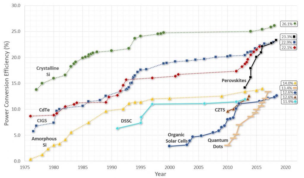
Fig. 1: Power conversion efficiency in solar cells. Courtesy of Ossila.

Lasers are already routinely used to investigate how light interacts with perovskites, spectrally and dynamically, on the micrometer scale. Compared to traditional light sources, lasers allow for the in-depth analysis that is needed to continue the flow of break-throughs in perovskite research. One of today’s challenges is to find the optimal composition of A, B, and X. The hunt is on…!

Efficiency mapping using a broad spectrum supercontinuum laser

It is critical to know how efficiently the perovskite crystals can absorb the different wavelengths of the solar spectrum. Such measurements can be carried out through photocurrent spectroscopy and imaging.

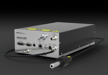
Our SuperK white light laser and SuperK VARIA filter offer the broad spectral coverage needed to investigate materials across the solar spectrum. The SuperK provides picosecond pulsed operation and a high-quality beam, allowing investigations of the optical properties with a diffraction-limited resolution. A set-up measuring absorption coefficient and refractive index can be seen in Fig. 4.

Understanding the structural properties with a picosecond pulse source

Structural properties, such as sample uniformity and defects, can help understand the limitations of the material. Here, hyperspectral imaging and exciton diffusion mapping can come in handy. The spectrum and picosecond pulse property of the SuperK white light laser supports the simultaneous acquisition of spectral and temporal data.

The unique properties of the SuperK laser allow you to have a picosecond pulse source at any wavelength in the visible and near-infrared spectrum. Combined with single-photon detection this allows for mapping of exciton lifetimes and diffusion lengths on a micrometer scale, unveiling exciton dynamics and defect densities only achievable through the versatility of the SuperK technology.

Example of perovskite researchers who have used our SuperK lasers and tunable filters in their set-ups

Professor Urban’s Nanospectroscopy Group, Ludwig-Maximilians University

Professor Urban’s group used the set-up in figure 2 to measure exciton lifetime.

The combination of a SuperK laser, a spectrometer, and a fast single-photon detector (an APD) made it possible to obtain spectral and lifetime information. High power enabled faster acquisition from the highly absorbing material.

A short cut-in wavelength was mandatory to get as close to the standard solar spectrum (e.g. ASTM G-173-03) as possible, making our SuperK FIU-15 or EXU-6 obvious choices.
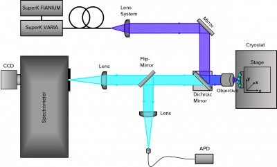
Figure 2: Courtesy of Professor A. S. Urban’s Nanospectroscopy Group.

Professor Urban’s group added cameras to the set-up in figure 2 to enable measurements of exciton diffusion lengths, see figure 3.
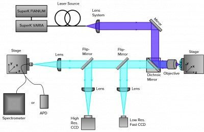
Figure 3: Courtesy of Professor A. S. Urban’s Nanospectroscopy Group.

Sarah Brittman and Erik C. Garnett, Center for Nanophotonics, FOM Institute AMOLF

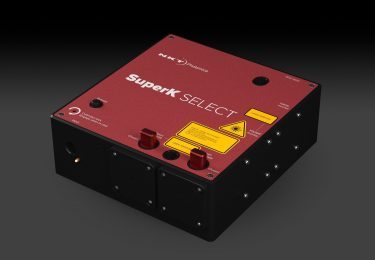
Sarah Brittman and Erik C. Garnett were performing refractive index and absorption coefficient imaging. Light from a supercontinuum laser was filtered by an acousto-optic tunable filter (the SuperK SELECT AOTF) and focused by an objective onto the sample, which was mounted on a piezostage.

Three photodetectors measured the incident, transmitted, and reflected beams at each wavelength produced by scanning the AOTF. A half-waveplate was used to control the laser’s polarization. A flip mirror, lens, and camera were used to image the sample to locate the crystals.
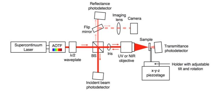
Figure 4: Refractive index and absorption coefficient imaging. Courtesy of Sarah Brittman and Erik C. Garnett.

The SuperK enables the following measurements

  • Pump-probe spectroscopy
  • Refractive index
  • Absorption coefficient imaging
  • Photoluminescence
  • Emission (exciton) lifetime; multidimensional
  • Quantum efficiency (IPCE vs QE); solar simulation
  • Single-photon counting

Papers on perovskite research using our SuperK white light laser


Typical examples are tiny single photonic components such as complex nano-waveguides, nano-apertures, and nano-resonators. Tight localization is of great practical importance, e.g. for high-resolution inspection, local modification of materials, high field concentration, intensity enhancement, increase of efficiency of nonlinear processes such as Raman scattering, and harmonic generation.

Nanoparticles of semiconductor materials arranged in bandgaps are called quantum dots. A quantum dot (QD) is a nanocrystal made of semiconductor materials that are small enough to exhibit quantum mechanical properties. Quantum dots are used in applications like solar cells, LEDs, and contrast agents in bio-imaging.

Publications

ARTICLES AND BACKGROUND INFO

Graphene is a single layer of carbon atoms held together by sp2 hybridized carbon atom bonds. Carbon nanotubes, essentially, are rolled-up sheets of graphene.

Examples of applications

Because graphene is such a strong material, it can be used to strengthen other materials. A sheet of graphene can be rolled up to form a carbon nanotube, which resembles a microscopic straw. Only, this straw is extremely thin and extremely strong at the same time.

Having zero effective mass, it does not add to the weight of the material it enhances. Obvious applications are building materials, aerospace, and others where lightness and strength are of the essence.

Graphene can also be used to spread heat due to its high electrical conductivity. This is especially useful in the microelectronics area, for strain sensors, supercapacitors, batteries that can recharge quickly, solar cells, and LEDs to name a few. It also makes it ideal for high-speed quantum physics experiments.

Due to its impermeability is can be used to filter water to get clean drinking water and graphene-based paint can prevent corrosion.

Use a SuperK supercontinuum laser to characterize graphene.

Get access to these techniques with our white light laser:

  • Fluorescence quenching microscopy
  • Scanning probe microscopy (SNOM/NSOM/STM/AFM)
  • Absorption spectroscopy/microscopy
  • Raman spectroscopy
  • Photoluminescence (PL) & photoluminescence excitation (PLE)
  • Surface plasmon resonance (SPR) adsorption spectroscopy
  • Rayleigh imaging and spectroscopy

Publications

The work listed below uses the SuperK supercontinuum laser from NKT Photonics to characterize graphene or carbon nanotubes.

What are nanostructures?

Nanostructures simply refer to physical structures with features on a nanometer scale. Structures relevant for optical characterization include such diverse fields as:

  • Metamaterials
  • Graphene and carbon nanotubes
  • Photonics bandgap structures
  • Surface plasmon waveguides
  • Nanofibers, spheres, rods, etc.
  • Quantum dots

How can I use a SuperK for nanostructure characterization?

Have you ever needed a different wavelength, wider tunability or a more convenient, stable or reliable light source? Then the SuperK white light laser is for you.

The SuperK advantages

  • Tune and interrogate any structure or resonance (380-2400nm)
  • Single-mode diffraction-limited output ideal for small structures
  • Stable power and excellent pointing stability of the beam
  • Active compensation for drift in setup via Power Lock
  • Reliable and easy to use with zero maintenance

The SuperK supercontinuum laser can give you light anywhere in the 380-2400 nm region, making it a great tool for the optical characterization of nanostructures. Many researchers around the World use the SuperK for measurements of nanoparticles, plasmonic waveguides, metamaterials, and other small structures.

The lasers are compatible with various characterization techniques like Raman spectroscopy, Brillouin light scattering spectroscopy, spectroscopic ellipsometry, SNOM, and s-SNOM which replace single-line lasers and traditional broadband sources.

Stability is the key

When characterizing very small structures, the stability of the light source is critical (e.g. for coupling to plasmonic waveguides).

As the only supercontinuum source on the market, the SuperK FIANIUM comes with our unique Power Lock feature that lets you lock the power anywhere in your setup. This lets you compensate for drift and instabilities in mirrors, lenses, etc., and gives you power stability at your sample in the 0.2-0.5 % range.

Power stability is important, but without good pointing stability of the beam, it is worthless. The SuperK FIANIUM has the best pointing stability on the market and is single-mode in the entire spectral range of the source.

You get a stable transmission through our filtering accessories but also a stable coupling to your sample resulting in less noise and better measurements.

Output through a SuperK VARIA with and without Power Lock. Power Lock improves stability to fractions of a percent.

A SuperK supercontinuum source can replace all of the following light sources:

  • ASE sources
  • Lamps
  • Single-line lasers
  • SLEDs
  • Dye lasers

ARTICLES AND BACKGROUND INFO