Materials processing of Nitinol

With its precise beam quality, adaptable pulse energy, and repetition rate, the aeroPULSE FS50 laser is ideal for Nitinol cutting for intricate arterial stents or bulk processing.

Nitinol is a highly unusual metal alloy of Nickel and Titanium. You can bend, twist, and crush it out of shape, only for it to jump back into its original shape when heated or submerged in hot water.

It possesses extraordinary super-elasticity and can survive repeated compressions and levels of repeated strain, whereas an equivalent piece of stainless steel will have long succumbed to fatigue.

Nitinol is nontoxic and does not promote genotoxicity, thus making it widely suitable for long-term medical implants.

The super-elastic properties of Nitinol coupled with its excellent biocompatibility means it has been the metal alloy of choice for demanding medical applications since the late 1980s.

Early medical uses of Nitinol include bone anchoring, tumor localization of specific cancers, and filter implants to trap and manage blood clotting. It is now widely adopted, with growing use, in minimally invasive surgery and dentistry.

The expected market growth for Nitinol in the medical market is expected to grow at over 9% CAGR, driven by improved therapy of chronic diseases and a preference for minimally invasive procedures. Nitinol is well suited to meet these needs.

Stents as an alternative to open surgery

Stents made from Nitinol are used to reinforce strictures within various ducts and canals of the human body caused by trauma or chronic medical conditions.

The use of stents negates any need to perform grafts or bypass surgery which makes it a highly desirable alternative to open surgery, where risks of secondary infection are higher.

Micromachined stent

Minimal thermal impact

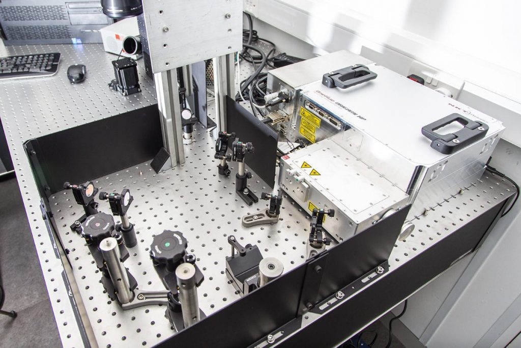
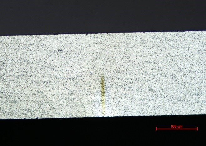
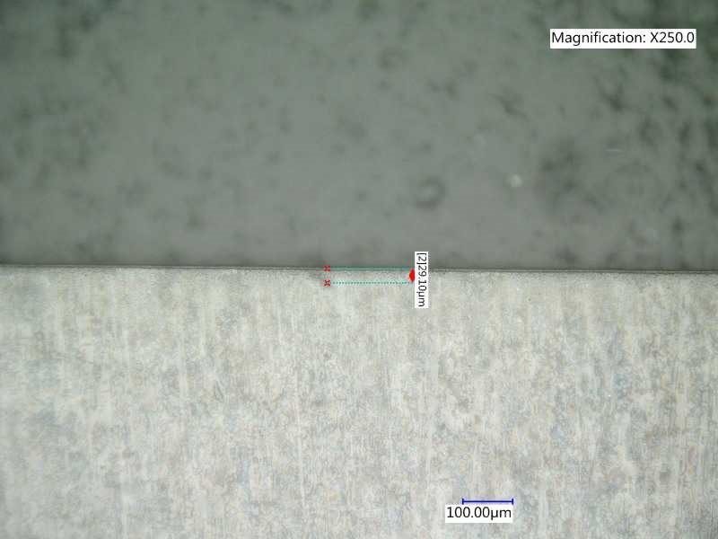
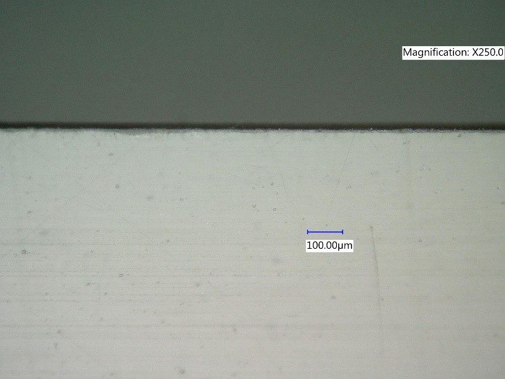
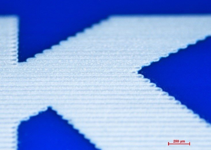
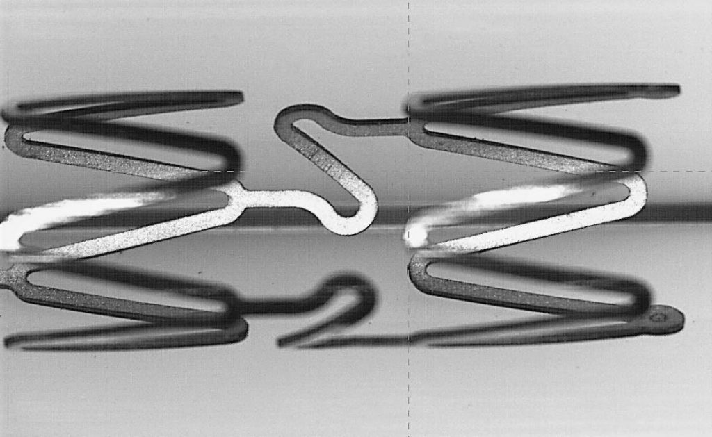
Ultrafast lasers are a natural choice to machine Nitinol stents and are widely used for this purpose. The near-diffraction-limited optical beam delivery yields a focused spot size optimized to machine small features. The short pulse dynamics of ultrafast lasers machine the Nitinol with minimal thermal stress or damage to the substrate.

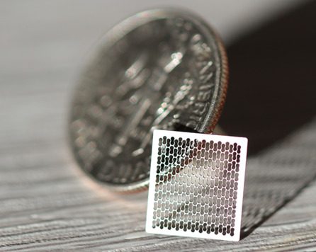
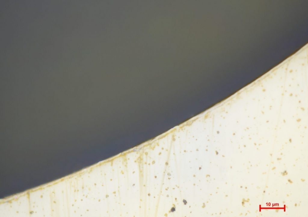
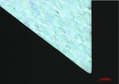
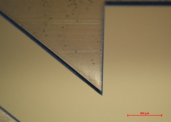
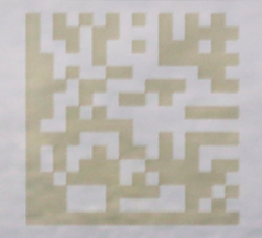
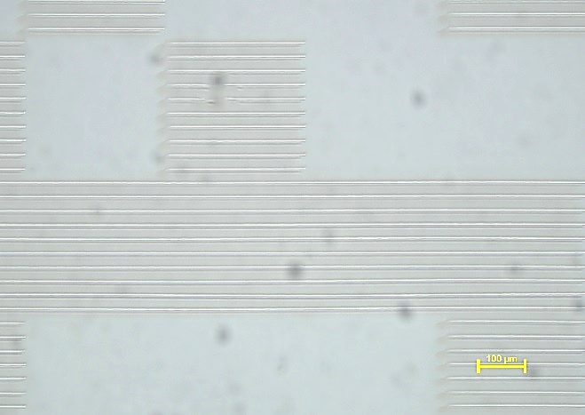
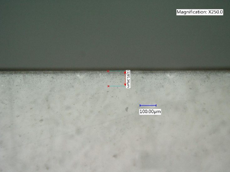
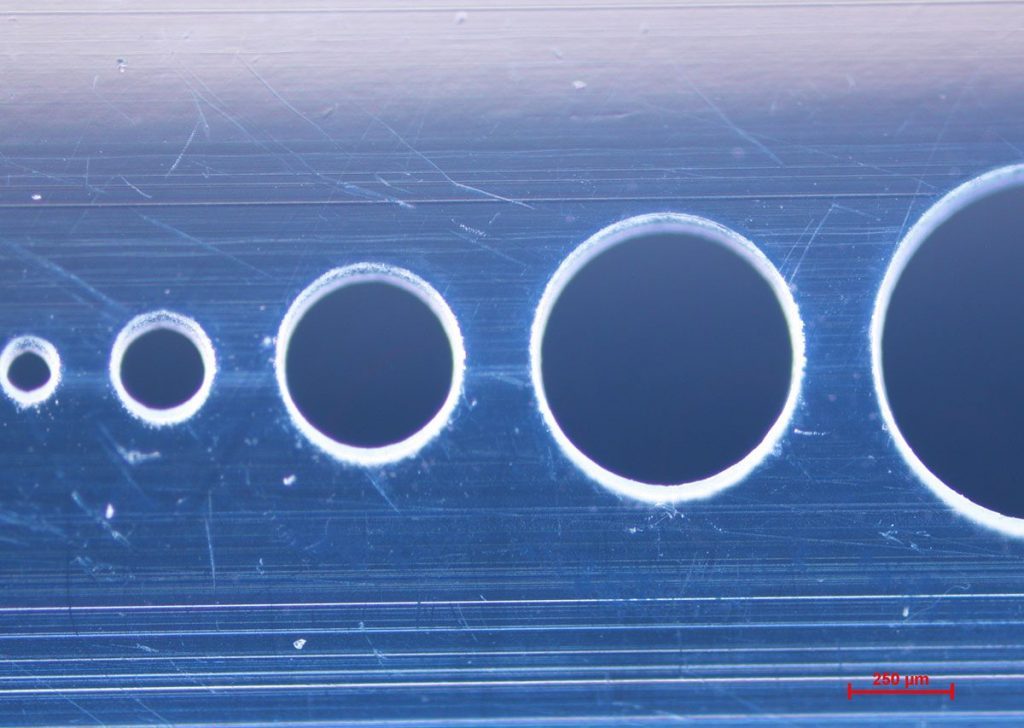
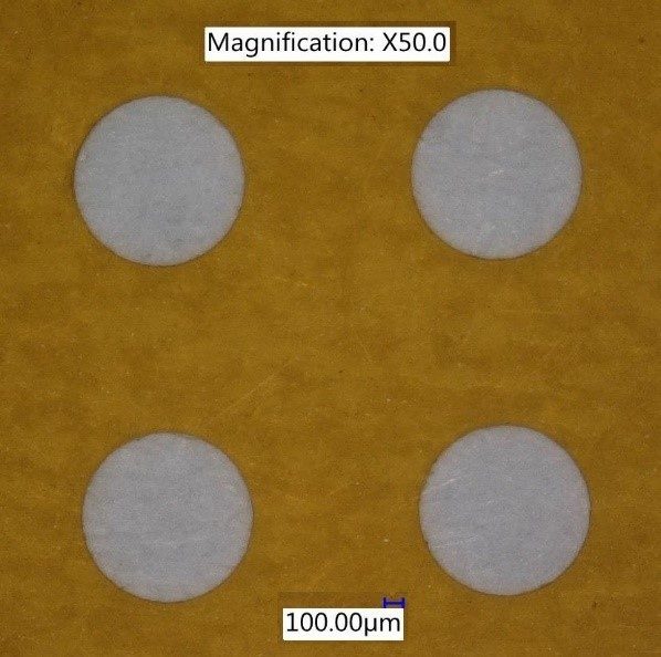
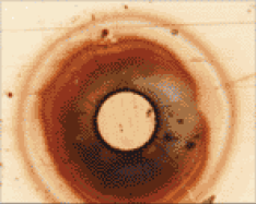
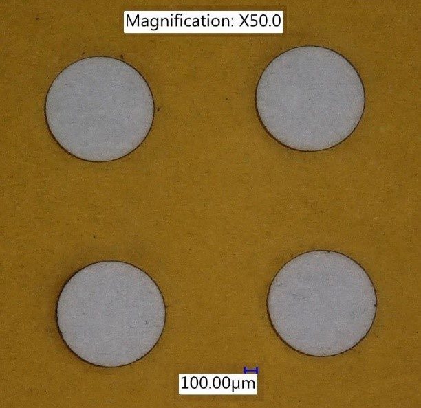
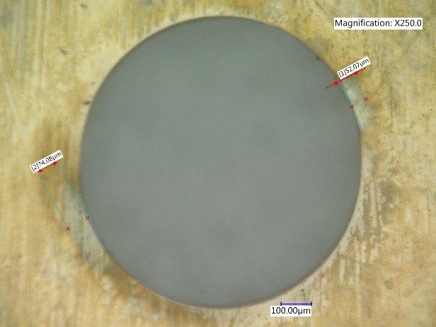
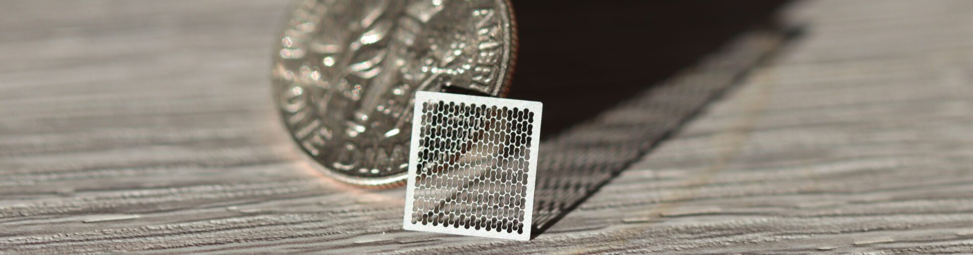
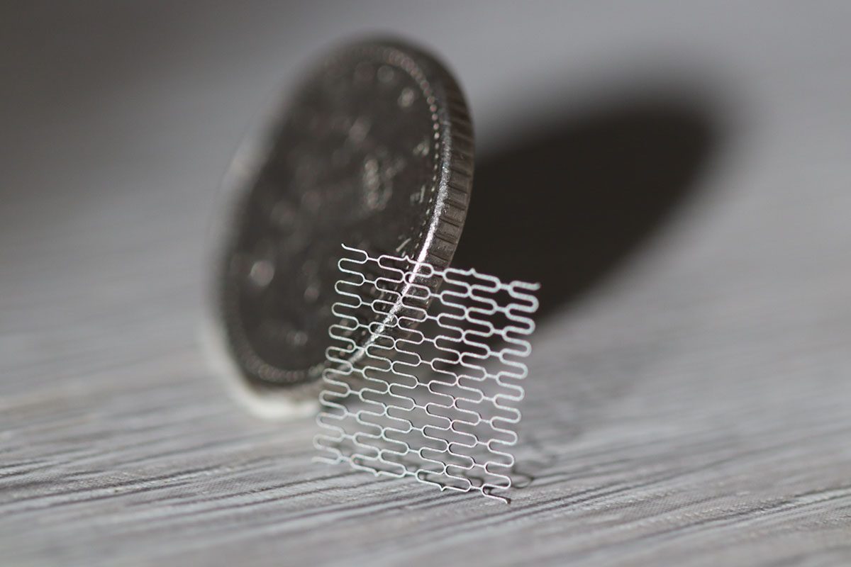
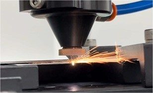
The test piece to the left shows the result of machining Nitinol with feature sizes consistent with an arterial stent. It was machined using our aeroPULSE FS50 laser using a single pass.

The laser beam was delivered using a commercially available processing head with an axial jet with a suitable cover gas to suppress oxidation and manage the generated plasma.

The results were an excellent simulation of the feature size and typical thickness of stents. The side walls are less than 65 µm and the feature sizes are <300 µm.

What lasers to use for Nitinol cutting?

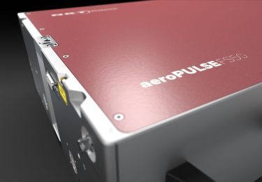
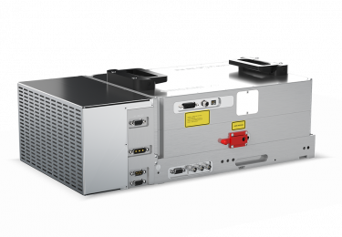
The aeroPULSE FS50 is an ideal laser for cutting Nitinol. The combination of near-perfect beam quality, pulse energy and repetition rate selection means that it can cut delicate features such as arterial stents but can also process larger stents or bulk Nitinol at higher speeds due to the option for higher repetition rate and average power.

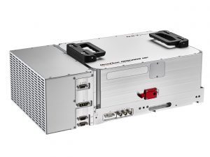
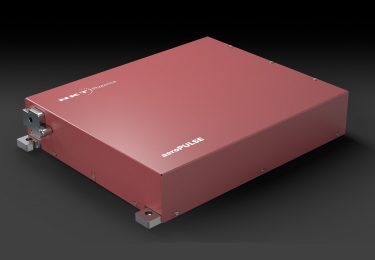
The aeroPULSE series of lasers is based on our photonics crystal fiber technology. As a result, it is an extremely reliable laser system ideal for industrial or scientific use. The FS50 is also used for cutting-edge neurostimulation research.

The ORIGAMI XP-S is also a strong candidate for Nitinol machining. Its excellent beam quality and high pulse energy are perfect for cutting fine features into Nitinol. The ORIGAMI laser is a diode-pumped solid-state laser architecture with a proven medical pedigree. It is used in a variety of biomedical applications, including ophthalmic laser surgery.

Both the ORIGAMI XP-S and the aeroPULSE FS lasers can be converted to different wavelengths via additional wavelength conversion units, which extend the range of materials they can process.

Both lasers also benefit from NKT Photonics’ powerful Software Development Kit (SDK), which can be used to independently control almost all laser output parameters.

Using the SDK, the laser, scanners, and stages can be automated to work together, enabling rapid research or production optimization. Both laser sources are ideal tools for basic R&D or full-scale volume production.

Download this application note as a pdf file.

ORIGAMI XP front

Let’s share the knowledge

We are continuously exploring the ultrafast processing of novel materials and are eager to share our knowledge to support your application development.

We can make tests and proof of concept in-house and apply our knowledge and skillset to your project, offering support and advice to enhance your results.

What do you want to do?

Regardless of your requirements, we are happy to offer advice and explore with you whether your laser micromachining requirements are ablation, drilling, cutting, glass cleaving, scribing, marking, engraving, welding, ophthalmology, opto-stimulation or surface functionalization of metals, ceramics, brittle transparent materials or organic materials.

Industry-leading equipment ensures the best result

Currently, we have two micromachining set-ups equipped with a wide range of galvo scanners, telecentric f-theta lenses, beam expanders, XYZ motion stages with a dual-axis position synchronized output (PSO) capability, various scanner control cards, and scanner software, and our versatile high-performance compact ultrafast lasers. With the right combination of optical components, we can focus laser beams down to a spot size of <5 µm.

Material processing is achieved with high accuracy, using nothing but industry-leading equipment from Aerotech, Newport, Zaber, Scanlab, Raylase, and NIKON. Furthermore, high-resolution CCD camera-based optical microscopy is employed to provide a detailed analysis of processed samples.

With a wide range of microscope objectives combined with the motorized XYZ stages and image stitching or automated Z-axis acquisition features, we can create a detailed 3D profile of features to analyze the results. If needed, access to SEM and TEM analysis equipment is available for exploratory material analysis.

Micro-machining for every industry

Our ultrafast lasers are capable to process virtually any material from metals, ceramics, glass, polymers, organic materials, and even composites. We can configure our setup easily to meet your micromachining needs whether you’re involved with display manufacturing, medical device manufacturing, automotive, aerospace, or semiconductor and microelectronics.

What can we explore for you?

Lab equipment

  • Galvo scanners
  • Telecentric f-theta lenses
  • Beam expanders
  • XYZ motion stages (dual-axis position synchronized output (PSO) capability)
  • A range of scanner control cards and software
  • High-resolution CCD camera-based optical microscopy
  • Our high-performance compact ultrafast lasers
  • Supporting optical components
  • Access to Scanning Electron Microscopy and Transmission Electron Microscopy

Address

NKT PHOTONICS LTD

20 Compass Point, Ensign Way
Southampton, SO31 4RA, UK

Laser cutting with short UV wavelengths gives several advantages:

  • Machine small volumes accurately with virtually no heat-affected zones.
  • Cut or drill thin polymer films or tubes into complex shapes with a high resolution.
  • High precision and low thermal input to the material due to small kerf widths.

Polymers are widely usedin manufacturingfor applications such as circuit boards, medical devices, OLED display technology, etc. Traditional mechanical processes tend to result in low yields and frequent retooling.

Laser processing of polymers is well-established. But, for markets that demand higher precision and quality or for thermally sensitive materials, a move to shorter wavelengths has gained wide acceptance in several industries. With the advantage of focusing to much smaller spot sizes than its longer wavelength rivals, a UV laser allows for material removal on much smaller scales over a wide range of materials. Furthermore, UV lasers are readily absorbed by most organic materials.

Combined with its shallow absorption depth, it is possible to precisely machine very small volumes with virtually negligible heat affected zones. Thin polymer films can be cut into complex shapes or drilled with exceptional resolution for applications within flexible circuit boards and OLED display technology.

Small kerf widths allow for higher precision and resolution whilst delivering much less thermal input to the bulk of the material, resulting in excellent quality cuts. The shorter wavelengths deliver longer Rayleigh lengths which give a bigger depth of focus for improved processing tolerances and can be utilized effectively when cutting non-flat samples, such as tubes.

In our applications lab, we have demonstrated the cutting of the following polymer films using our ORIGAMI-03XPUV femtosecond laser:

• PET

• PTFE

• COC

• Polycarbonate

Kaptonfoil (25μm thick) cut with ORIGAMI-03XP343nm laser.

Kapton (polyimide) is well-known for its ability to retain its mechanical, electrical, and thermal properties under harsh conditions as well as its chemical inertness and is widely used in flexible circuits. The ORIGAMI-03XP UV laser cuts these films with exceptional cut quality.

PET cut with ORIGAMI-03XP343nm laser.

Polyethylene terephthalate (PET) film is a clear, strong, and lightweight material. It is becoming a popular substrate in the consumer electronics industry for manufacturing flexible microelectronics circuits and displays due to its transparency, high tensile strength, thermal stability, electrical insulation, and chemical resistance properties.

PET is often used in OLED display manufacturing and frequently stacked with other materials. The 75 μm thick sample is transparent, but this is no problem for the ORIGAMI-03XP laser.

PET is prone to thermal damage, so the ORIGAMI-03XP UV laser provides a solution that cuts these films with minimal heat leading to excellent cut quality and high precision.

PTFE150μm thick cut using the ORIGAMI-03XP laser

PTFE has good electric insulation properties and is used to insulate cables and connector assemblies.

Combined with its chemical inertness and low refractive index, it is ideal for the microelectronics industries exhibiting displays and flexible printed circuit boards.

Co polymers/COC are low-cost polymers with a high optical transparency, chemical resistance, and bio-compatibility. It is a glass-clear and extremely pure plastic for healthcare, optics, packaging, and electronics applications.

Polycarbonate films are well known to offer good optical clarity, very high impact strength, and offerresistance against high temperatures for distortion.

COC100μmthick cut with high precision and good quality using the ORIGAMI-03XP UV laser.
LEXAN polycarbonate 125μm thick filmcut using the ORIGAMI-03XP UV laser.

Summary

The ultrashort pulses delivered by the ORIGAMI-03XP UV laser are very well suited for processing thermally sensitive polymer films which are often used in display or electronics. The low HAZ and small spot size afforded by the ORIGAMI-03XP ensure precision machining with high quality.

ONEFIVE ORIGAMI 03XP

The ORIGAMI-03XP is a UV femtosecond laser, allowing computer-controlled, flexible switching between IR, green,or UV wavelengths in one laser system.

Based on the highly successful ORIGAMI XP platform, the same advantages of clean, femtosecond pulse output, excellent beam quality together with unprecedented beam stability are obtained as a result of the OptocageTM laser design.

Download this application note here.

The high peak powers produced by femtosecond laser pulses allow successful precise laser sub-surface marking within transparent materials, such as glass.

This is important in applications where product traceability, product branding, and more importantly, anti-forgery require tamper-free and permanent marks. Sub-surface marking renders the actual surface uncompromised and debris-free.

The contrast of the marks can be made high or subtle by fine control of the laser processing parameters. Typically, surface marking of glass is achieved using ns pulses at 1064 nm, such as CO2 or fiber lasers.

These lasers mark the glass material by generating fractures at the surface. When using long pulse lasers (ns), thermal reactions form micro-cracks, the marking becomes visible. Other methods employ single-photon green or UV ns lasers, but this can still lead to unwelcome thermal effects which can compromise the desirable properties of the glass.

Transparent materials are notoriously difficult to mark using conventional lasers. Such markings produce debris when machining the surface. By focusing a 1030 nm femtosecond beam tightly into the bulk of the glass, it is possible to absorb multiple photons leading to a highly localized mark inside the glass lattice with negligible heat input.

Very small features can be achieved inside the glass lattice and the surface remains unaffected, making the marks impervious to chemical cleaning. The short pulse widths ensure that the thermal load into the sample is virtually inconsequential, so chipping and fracturing of the sample are insignificant.

The interaction of the laser with the glass lattice produces permanent structural modification by altering the refractive index that gives rise to a contrast marking which can be seen by the eye. Since the mark exists under the surface, it cannot be removed or altered.

Debris-free sub-surface marks on a glass microscope slide made using our ORIGAMI XP IR laser.

It is essential to focus the beam to a small spot size within the glass to avoid surpassing the damage threshold fluence on the surface. Marking of inside the crystal requires fine adjustment of the focus position combined with small spot sizes to reach a fluence that surpasses the damage threshold inside the desired area of the crystal.

By focusing the beam tightly, it is possible to control the depth of the marking whilst ensuring that the fluence at the surface is not above the damage threshold in unwanted planes.

Microscope image of a sub-surface line. The marking is free of debris and defects and the surface is unaffected.
Varying parameters to show different contrasts.

Conclusion

In our applications lab, we have demonstrated the sub-surface marking of glass slides using the ORIGAMI 10XP femtosecond laser. The clean soliton-like femtosecond pulses ensure precision delivery of peak power to create the internal marks and the excellent beam quality of the laser ensures a tightly focused spot, allowing good depth control of the mark’s location. By adjusting the pulse spacing or number of passes, it is possible to enhance the contrast for a more readable mark, or where needed, to produce a more subtle mark for anti-counterfeit applications.

Summary

The ultrashort pulses delivered by NKT Photonics’ ultrafast laser range are well suited to producing sub-surface marks in glass. This was demonstrated successfully with the ORIGAMI 10-XP laser.

ONEFIVE ORIGAMI XP

The ORIGAMI XP is the first all-in-one, single-box, microjoule femtosecond laser on the market. The laser head, controller and air-cooling system are all integrated in one small and robust package, with a footprint so small it even fits into a hand-luggage!

The ORIGAMI system is based on a compact monolithic chirped pulse amplification platform capable of delivering up to 70 μJ pulse energy at 1030 nm, a 5 W average power, and a pulse duration below 400 fs.

Download this application note here.

Polyethylene terephthalate (PET) film is a clear, strong, and lightweight material.

It is becoming a popular substrate in the consumer electronics industry for manufacturing flexible microelectronics circuits and displays due to its transparency, high tensile strength, thermally stability, electrical insulation and chemical resistance properties.

Compared to glass and other flexible substrates, PET is a low-cost solution. Maybe you know PET as Mylar, Melinex, or Hospaphan?

Low-cost, low-weight, and high flexibility

The use of flexible substrates significantly reduces the weight of flat panel displays and provides the ability to conform, bend, or roll a display into any shape. It opens the possibility of fabricating displays by continuous roll processing, making mass production highly cost-effective. In some cases, it even allows printing circuits onto the substrate instead of using an expensive physical material deposition process.

Avoid thermal load

As displays are getting thinner and lighter with higher functionality, they demand the fabrication of precise small features. Laser micromachining is an ideal solution to create such tiny precise features in any material. One of the main challenges in laser machining of PET film is its low glass transition temperature of 78°C. It is essential to avoid any process that adds thermal load into the material and form blisters that can deform the material significantly.

It is not possible to machine PET film using long pulse nanosecond lasers due to the thermal load that long pulses deliver to the material. Ultrafast femtosecond lasers, on the other hand, provide a non-thermal cold ablation process due to their short pulses with high peak power, which makes them ideal for the micromachining of PET film.

High-quality micromachining of PET film

Figure 1. 800-micron diameter multi-pass trepanned-drilled array of holes using our ORIGAMI XP IR laser

In our application lab, we studied the cut quality of PET films, using our ORIGAMI XP femtosecond laser.

Figure 1 shows a thin 75-micron PET film micro-machined using our ORIGAMI XP femtosecond laser. We created an 800-micron diameter multi-pass trepanned-drilled array of holes using the infrared wavelength.

As expected, we achieved a clean-cut hole in the PET film. The instant removal of material with high peak-power short pulses indeed provides a clean melt-free material removal.

A closer evaluation of a straight-line cut, see Figure 2, shows the redeposition of loose dust near the cut edge, creating a dust zone of ≈95 microns extending from the cut edge.

Figure 2. Redeposition of loose dust created a dust zone of ≈95 micron extending from the cut edge.

Based on our experience of machining plastic films using femtosecond lasers, we expected to achieve a better cut quality using a green wavelength laser. We made the straight-line cut, shown in Figure 3, using the ORIGAMI 05XP green laser. It did indeed show improvement in the cut quality, with a reduced dust zone of ≈29 microns.

We were further able to get rid of the dust zone by simple alcohol swab cleaning. We ran an alcohol swab across the infrared wavelength cut sample surface from Figure 1. The result was a very clean cut edge, Figure 4.

Figure 3. Improved cut quality and a dust zone reduced to ≈29 micron using our green wavelength ORIGAMI XP laser
Figure 4. We removed the dust with a simple alcohol swab to get a clean cut edge.

Conclusion

The results show that our ORIGAMI XP femtosecond laser is well-suited to machine PET films. We have demonstrated that both infrared and green wave-lengths can process PET films with high-quality edges. A green wavelength improves the cut quality even further by reducing the dust zone. If a dust-free cut is required, a simple alcohol swab can remove any loose dust created during machining.

Summary

The ORIGAMI XP laser delivers clean, ultrashort femtosecond pulses which is ideally suited for the precise machining of thermally sensitive materials, such as PET film.

ORIGAMI XP

The Origami XP is the first all-in-one, single-box, microjoule femtosecond laser on the market. The laser head, controller and air-cooling system are all integrated in one small and robust package, with a footprint so small it even fits into a hand-luggage!

The ORIGAMI XP system used in this study is based on a compact monolithic chirped pulse amplification platform capable of delivering up to 40 μJ pulse energy at 1030 nm, a 4 W average power, and a pulse duration below 400 fs. Also available is the Origami XPS is delivering up to 5W and 70uJ at 1030nm with green and UV capability.

Download the application note here

A high contrast mark has been made on a blue nylon tube using our ORIGAMI 10XP. Alphanumeric characters, logos, and barcodes are all achievable.

Laser marking offers the flexibility to directly mark a range of alphanumeric characters, logos, images, or barcodes on polymers without contact with the sample.

Materials processing with ultrafast lasers provides unique advantages over conventional laser processing techniques that typically employ nanosecond and longer pulses.

Fast high-precision processing

The short pulse widths and high repetition rates of ultrafast lasers allow for faster processing speeds – with high precision – giving rise to the possibility of creating incredibly small marking features compared to longer pulse durations marking.

The multiphoton absorption of ultrashort pulses means that the wavelength of the femtosecond pulses plays a less critical role and in the cold processing regime, the marks are free of melting and charring.

Nylon tubing is widely used in manufacturing of medical devices because of its lightweight, corrosion, and abrasion resistance.

High-quality marks on transparent samples

Ultrafast lasers can be used to process a number of polymers, irrespective of transparency or thickness. The same laser that can cut the material, can also produce a permanent, high-quality mark, simplifying manufacturing by enabling more than one process by a single laser. In most cases, the quality of such cuttings and markings eliminate the need for post-processing and reduces the manufacturing cost.

Marking of medical devices

At NKT Photonics we have recently completed a study of marking various polymer tubes that are commonly used in medical device manufacturing.

Polyimide is a high-performing polymer commonly used in implantable medical device manufacturing since it is fully biocompatible.

Here, a high contrast mark has been produced on a 1.7 mm diameter tube. Precise, fine features are easily achieved with ultrafast lasers.

The ORGIAMI 10XP laser can process a wide range of polymers, producing high quality and high contrast
marks that are both human readable and machine readable.

Polyimide tube has been marked using
our ORIGAMI 10XP laser.

PTFE tube

PTFE is commonly used in the medical industry. It offers usage up to high temperatures, excellent non-stick properties due to its low coefficient of friction, good abrasion resistance, chemical inertness, excellent dielectric stability, and excellent wear resistance.

PTFE tube has been marked using our
ORIGAMI 10XP laser.

Summary

The Ultrashort pulses delivered by NKT Photonics’ ultrafast laser range are well suited to precision marking fine features onto a wide range of polymers that are frequently used within the medical device manufacturing industry.

The Origami XP is the first all-in-one, single-box, microjoule femtosecond laser on the market. The laser head, controller and air-cooling system are all integrated in one small and robust package, with a footprint so small it even fits into a hand-luggage!

The ORIGAMI system is based on a compact monolithic chirped pulse amplification platform capable of delivering up to 70 μJ pulse energy at 1030 nm, a 5 W average power, and a pulse duration below 400 fs.

Download this application note as pdf.

As medical devices develop and get smaller, the ability to make high-quality cutting and fine features become more important.

With high peak-power ultrafast lasers, you can make high-quality fine features without any thermal effects.

In recent years, the use of ultrafast lasers to fabricate polymer medical devices has gained wide acceptance due to the lasers’ ability to create fine, precisely machined features and markings. Unlike mechanical methods of polymer cutting, a laser cut is a non-contact process without any tool wear which ensures a consistently high-quality cut. The transition from mechanical processing to laser machining was primarily driven by the need to create very small precise features at a high yield and lower cost.

Cut and mark in one process

Ultrafast lasers can process a wide variety of polymers, regardless of transparency or thickness. You can use the same laser to cut fine features and to produce permanent, high-quality marks. This way, you simplify manufacturing since one laser can do more than one process. The high-quality cutting and marking eliminate the need for post-processing and reduce the overall manufacturing cost.

Cold ablation ensures precise, debris-free features

The duration of laser pulses has a dramatic effect on laser cutting results. When the pulse-duration is below some tens of picoseconds, the laser-material interaction enters the “cold” or “athermal” ablation regime. The cutting quality significantly improves by breaking down the material instantly in a precise manner, while the surrounding material is unaffected.

In our applications lab, we have demonstrated the cutting of various polymer tubes using our ORIGAMI 10XP femtosecond laser.

200 µm wall blue nylon tube cut using our ORIGAMI 10XP laser.

Nylon tubing is ideal for medical devices because it is lightweight, corrosion and abrasion resistant. It can withstand repeated stress over extended periods. Its strength, crush, cracking and tear resistance makes nylon perfect as the outer jacket of catheters.

Typical uses: Structural heart, peripheral, general medical, endovascular, cardiovascular, cardiac rhythm management/electrophysiology.

Polyimide tube

Polyimides are a family of high-performing polymers. They are particularly known for their mechanical performance and their chemical resistance.

Polyimides exhibit exceptional thermal stability throughout high and low temperatures and excellent insulating performance through a range of environments and frequencies. In addition, they are also known for their high strength and exceptional tensile strength.

50 µm wall polyimide tube using our ORIGAMI 10XP laser.

These properties, and more, have led to widespread use of polyimide in the medical, aerospace, automotive, and electronics industries. Since polyimides are fully biocompatible, polyimide tubing can be used for both vascular and urinary catheter constructions. With its extremely small sizing capabilities, polyimide tubing can be produced to reach the smallest sized vasculatures while retaining strength and rigidity.


Typical uses: Polyimide tubing with its small sizing capabilities can be used for both vascular and urinary catheter construction.

150 µm wall PTFE tube using our ORIGAMI 10XP laser.

Polytetrafluoroethylene (PTFE) liners are commonly used at the heart of catheters. The combination of extremely thin walls and the material’s superior lubricity make it the ideal material for catheter liners.

PTFE is a good fit for the medical industry; it offers usage up to high temperatures, superior non-stick properties due to its low coefficient of friction, good abrasion resistance, chemical inertness, out-standing dielectric stability, and excellent wear resistance.

Typical uses: Cardiovascular, endovascular, structural heart, cardiac rhythm management / electrophysiology, peripheral, general medical.

Summary

The ultrashort pulses delivered by our ultrafast laser are well suited to precision cutting of polymer tubes.

The Origami XP is the first all-in-one, single-box, microjoule femtosecond laser on the market. The laser head, controller and air-cooling system are all integrated in one small and robust package, with a footprint so small it even fits into a hand-luggage!

The ORIGAMI system is based on a compact monolithic chirped pulse amplification platform capable of delivering up to 70 μJ pulse energy at 1030 nm, a 5 W average power, and a pulse duration below 400 fs.

Download this application note as pdf.

Polyimide (or PI or Kapton) is a thin film widely used in the medical and microelectronics industries due to its mechanical strength, electrical insulation, thermal stability, chemical inertness, and biocompatibility. 

Ultrafast lasers provide the needed precise, non-contact micromachining processing technique with a minimal need for post-processing.

Good for medical and microelectronics industries

Polyimide (or PI or Kapton) is widely used in the manufacturing of microelectronic components for the semiconductor, computer, automotive, aerospace, and display industries. It is popular due to its mechanical strength, electrical insulation, and thermal stability. In microelectronic components, polyimide is used in wafer carriers, test holders, hard disk drives, electrical connectors, wire insulators, flexible printed circuit boards, digital copier and inkjet printer components. Due to its chemical inertness and biocompatibility, polyimide is used increasingly in medical applications such as the manufacturing of cardiovascular catheters, retrieval devices, push rings, marker bands, angioplasty, stent delivery devices, neurological devices, and drug delivery systems.

Increase miniaturization and avoid post-processing

If you work in the semiconductor or medical device industry, you know the importance of manufacturing lighter, smaller, higher-density, and higher-functionality products to meet market demands. You need to find ways to make a wide range of tiny and precise features. In the early days, nanosecond pulse-width ultraviolet (UV) lasers made it possible to create small precise micron-size features in polyimide film. However, the big drawback of long nanosecond pulse UV lasers is the black carbon shoot debris that is generated around the ablated machined features1.

Figure 1. Typical surface debris around the features left behind by nanosecond UV laser

Two challenges are

1) it is necessary to post-process the sample to remove the surface debris which adds to the overall cost

2) there is a limit to how closely you can machine two features, which limits the density of features and the degree of product miniaturization.

It is well-known that ultrafast femtosecond laser pulses ensure clean debris-free metal removal. We wanted to explore if our ORIGAMI ultrafast laser could perform equally debris-free machining when it came to the ablation of polyimide film.

Trepanning using IR and green wavelength lasers

The first set of experiments was conducted using our ORIGAMI IR wavelength laser. With a multi-pass process, we trepanned large 1 mm diameter holes in a 25 µm thick polyimide film using a 20 µm diameter focused laser beam.

We observed a large decrease in debris-generation compared to nanosecond pulse UV laser machining. The high peak-power of the femtosecond laser pulse pulverizes the material instantly and leaves the surface debris-free.

So, if you want to decrease debris-generation during machining of polyimide, one of the ways is to use a high peak-power femtosecond laser.

Figure 2. Trepanned holes drilled using ORIGAMI IR laser.

Upon further higher-magnification inspection of the holes, we did observe a small heat-affected zone (HAZ) of ≈ 52 to 74 µm around the edges of the hole.

Figure 3. HAZ around ORIGAMI IR laser machined hole.

We extended our study further to explore the reduction of HAZ in polyimide machining using a green wavelength laser.

A multi-pass trepanning hole drilling using a green wavelength ORIGAMI laser gave us holes with virtually no HAZ

Figure 4. Trepanned holes drilled using ORIGAMI green laser.
Figure 5. Clean debris-free surface with no HAZ, machining achieved using green wavelength ORIGAMI laser.

We verified the debris-free surface by higher-magnification inspection and confirmed non-existent HAZ as shown in Figure 5.

Conclusion

Our results indicate that our ORIGAMI femtosecond laser can be used to achieve a debris-free no-HAZ machining of polyimide film. The higher peak power of femtosecond laser pulses indeed helps to vaporize polyimide film instantly, leaving a debris-free surface.

Summary

Our results demonstrate that femtosecond pulses, delivered by our ultrafast lasers, are well suited for debris and HAZ free micromachining of polyimide film.

The ORIGAMI XP is the first all-in-one, single-box, microjoule femtosecond laser on the market. The laser head, controller and air-cooling system are all integrated in one small and robust package, with a footprint so small it even fits into a hand-luggage!

The ORIGAMI system is based on a compact monolithic chirped pulse amplification platform capable of delivering up to 70 μJ pulse energy at 1030 nm, a 5 W average power, and a pulse duration below 400 fs.

1 https://www.laserfocusworld.com/software-accessories/positioning-support-accessories/article/16552519/excimer-lasers-drill-inkjet-nozzles

Download this application note as pdf.

Since their introduction in 1986, stents have transformed the treatment of coronary heart disease.

By 1999, stent-based surgeries accounted for 84% of all percutaneous coronary interventions (PCIs). Laser cutting was used in coronary stent fabrication almost from the start.

Laser cutting with nanosecond pulsed infrared (IR) lasers easily met the accuracy requirements for large feature machining of stainless-steel stents in the early days. However, the thermal nature of nanosecond laser ablation resulted in poor cut-edge quality. This called for costly cleaning, deburring, etching, and final polishing to bring the stent’s edge quality to the level and consistency required for implantable devices.

Fine-feature demands call for ultrashort pulse lasers

When stent material transitioned from stainless steel to nickel-titanium and then to high-strength superalloys with more challenging fine-feature requirements it became necessary to use ultrashort pulse (USP) lasers to avoid the thermal nature of machining. The migration to drug-eluting and later bioresorbable stent technology boosted the adoption of USP laser technology.

Third-generation bioresorbable stent (BRS) technology further accelerated the implementation of USP laser machining in stent manufacturing. The scaffolding in BRS technology is made from biodegradable polymers. The polymers gradually dissolve in the body making them less intrusive than metal scaffolding while helping to reduce the occurrence of blood clots and other ill effects.

High-quality USP micromachining

The duration of laser pulses has a dramatic effect on laser micromachining results. When pulse duration is below some tens of pico-seconds, the laser material interaction enters the “cold” or “athermal” ablation regime and the machining quality improves significantly.

While the advantages of ultrafast laser-material interaction physics are clear, the commercial viability of USP lasers was not so obvious until recently, when a robust alternative to classic Ti:sapphire gain media emerged.

At NKT Photonics we have put tremendous effort into developing the ORIGAMI XP laser – the first all-in-one, single-box, microjoule femtosecond laser on the market.

The laser head, controller, and air-cooling system are all integrated into one small and robust package, with a very small footprint.

Recently, we have demonstrated cold ablation of nitinol stent cutting using an Origami XP laser and have achieved a very high cut quality.

Summary

The Ultrashort pulses delivered by NKT Photonics’ ultrafast lasers are well suited to micromachine a lot of different stent materials. Lasers are extremely reliable in creating the precise fine features demanded by today’s state-of-the-art stent designs cost-effectively.

The Origami XP is the first all-in-one, single-box, microjoule femtosecond laser on the market. The laser head, controller and air-cooling system are all integrated in one small and robust package, with a footprint so small it even fits into a hand-luggage!

The ORIGAMI XP laser is based on a compact monolithic chirped pulse amplification platform capable of delivering up to 70 μJ pulse energy at 1030 nm, a 5 W average power, and a pulse duration below 400 fs.

Download this application note as pdf