We take for granted that our new smartphone is faster than its predecessor. It is thinner, has more capacity, and a highly responsive, crystal-clear touch screen. In a few years, you might even be able to roll it up and put it in your pocket. We anticipate renewable energy from the sun and wind to become more efficient and profitable. We expect that electric cars and trains will play a major role in our sustainable society and our environment in the future.
The semiconductor industry is one of the driving forces behind this development. It delivers processing power to handle astronomical amounts of data and efficient components for high-power electronics.
Terahertz radiation measurement technology
A new project, TRIM, aims to develop optical technology based on terahertz radiation. The new technology can measure the quality of electric and magnetic materials and ensure high-quality materials and homogeneity for the semiconductor industry. TRIM is short for Terahertz Resistivity Imaging. The project has a total budget of DKK 27 million and is backed by the Innovation Fund Denmark with DKK 19 million.
Faster, bigger, better…
“Some of the keywords for the continued development of a sustainable information society are: Greater speed, larger storage capacity, and higher reliability – all are features that depend on control and quality assurance. For many years, the terahertz technology has been the focus of research around the world – now it is time to bring the huge investments in fundamental research into the real world and see it prove its worth,” says Professor Peter Uhd Jepsen from the Department of Photonics Engineering, the Technical University of Denmark. Professor Jepsen will lead the project in the coming three years.
Touch-free characterization
The terahertz technology enables a unique way to perform complete touch-free measurements – something that is certainly needed in the industry – and an important requirement for characterization of e.g. 2D materials consisting of a single or very few layers of atoms.
The development of the Terahertz Resistivity Imaging technology takes place in close collaboration between the Technical University of Denmark and the companies Capres A/S, Topsil GlobalWafers A/S, and NKT Photonics A/S. The project connects world-leading competencies within terahertz and laser technology, silicon production, and characterization of semiconductor materials. The project introduces completely new technology and methodology to an industry known to be particularly conservative and cautious.
Denmark at the forefront
“Denmark has a strong history within the characterization of materials for the semiconductor industry, but there is still some way to go to move the experience from the labs into the industry. This investment from the Innovation Fund Denmark will help us overcome the natural technological and commercial barriers that must be broken down to accept new technologies and methods, “says Peter Uhd Jepsen.
Three of Denmark’s leading semiconductor companies participate in the project and they see great opportunities in getting direct access to world-leading research:
Capres A/S
“Capres A/S expects the TRIM project to significantly expand the market potential for the sale of advanced, fully automated machines to existing as well as new customers in the semiconductor industry. Combining our unique multi-pin, nano and micro probe-based measurement technique with the new contact-free optical measurements will expand the scope and measurement speed in the areas of material characterization, process optimization, and process control.”
CTO & Co-Founder Peter Folmer Nielsen
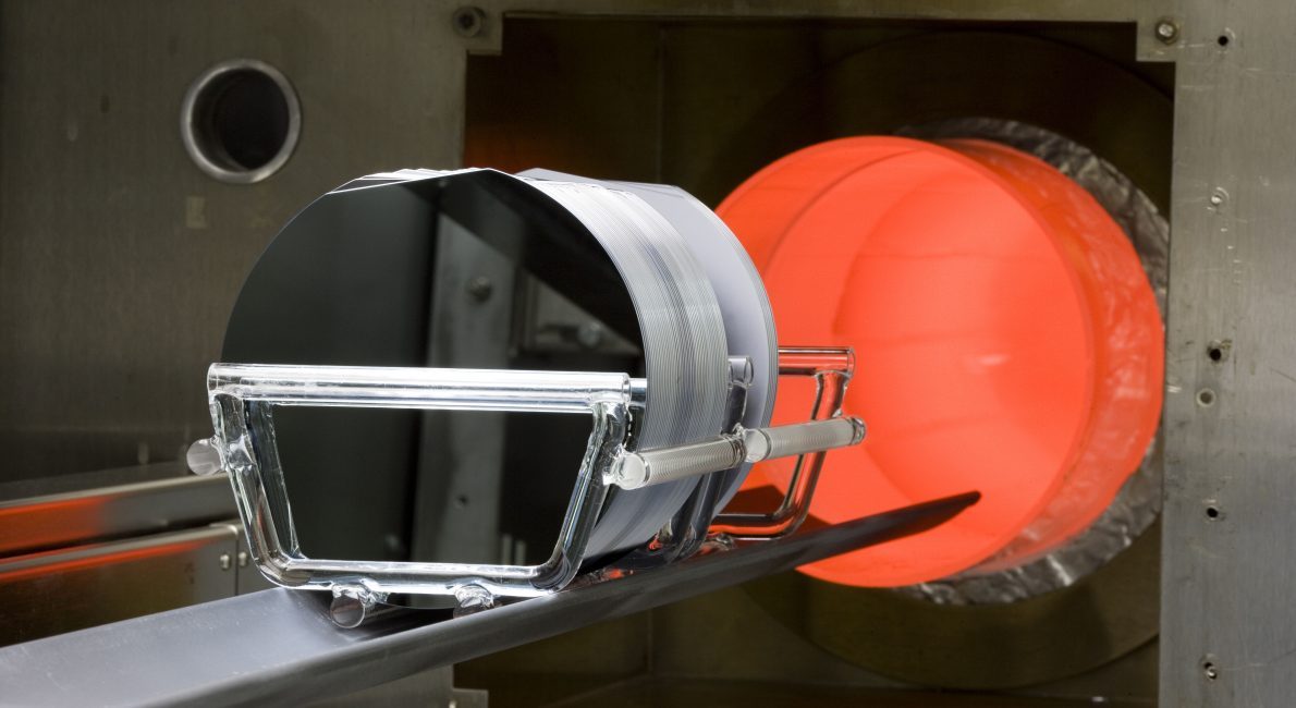
Topsil GlobalWafers A/S
“For Topsil GlobalWafers A/S, the project results in improved process control and more precise characterization of our products. The improved process control and, consequently, increased productivity allows Topsil to stay competitive against companies with production in low-wage countries.”
Development Manager Sune Bro Duun
NKT Photonics A/S
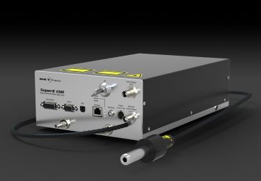
“A large part of NKT Photonics’ success originates from the fact that we have been at the forefront of the technological development right from the start. The TRIM project is an obvious example of how technology under development has the potential to make the Danish high-tech industry a key supplier to the extensive semiconductor industry. Within TRIM, NKT Photonics’ role is to develop and deliver the laser systems. The phase noise requirements are extremely strict, but we happen to have the market’s most suitable laser.”
Principal Research Scientist Peter Moselund, NKT Photonics A/S
The lasers used in the project are two ORIGAMI 15s from NKT Photonics A/S.
About the project
- Project title: TRIM: Terahertz Resistivity Imaging
- Total budget: DKK 27 million
- Investment from Innovation Fund Denmark: DKK 19 million
- Duration: 3 years
Contact information
Technical University of Denmark, Professor Peter Uhd Jepsen, +45 5115 7408
Innovation Fund Denmark, Communications Manager, Thomas Bjerre, +45 6190 5019
Capres A/S, CTO Peter Folmer Nielsen, +45 2363 8313
Topsil GlobalWafers A/S, Research and Development Manager Sune Bro Duun, +45 5192 6671
NKT Photonics A/S, +45 4348 3900