The FDA requires that all medical devices are marked with a Unique Device Identifier (UDI).
The marking must have lifelong durability to ensure traceability and patient safety.
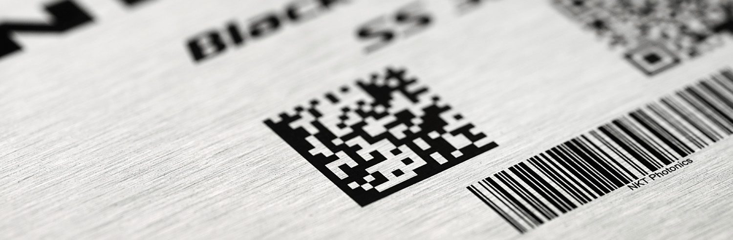
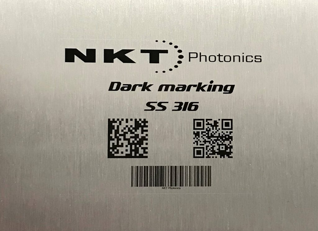
It must contain plain text which is readable by humans as well as machine-readable code. Both must be permanently legible because traceability is crucial for medical implants and surgical devices. An ultrafast laser provides a smooth mark with high contrast.
Marking of all kinds of material
Medical devices can range from implants and catheters to less invasive multi-use surgical tools such as scissors, forceps, and scalpels.
Typical materials that are used in the manufacture of medical devices are:
All can be marked using our ultrafast lasers.
Cost-effective permanent marking
Most marks are required to remain durable after regular use and cleaning, which makes laser marking ideal.
Laser marking is an attractive and cost-effective marking solution with many advantages: The process reliability, the non-contact nature, the inherent flexibility, the capability to create intricate details, the micron precision. And there is no need for consumables.
Why use ultrafast lasers?
Ultrafast lasers have many advantages compared to nanosecond lasers. You can mark a wide range of materials due to the short pulse duration that gives a high peak power. The short pulse duration reduces the unwanted thermal effects of traditional laser marking.
Medical device markings must repeatedly withstand the high temperatures and humidity of autoclave cleaning and sterilization. Conventional thermal laser markings typically fade or corrode when cleaned frequently.

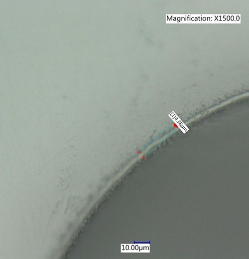
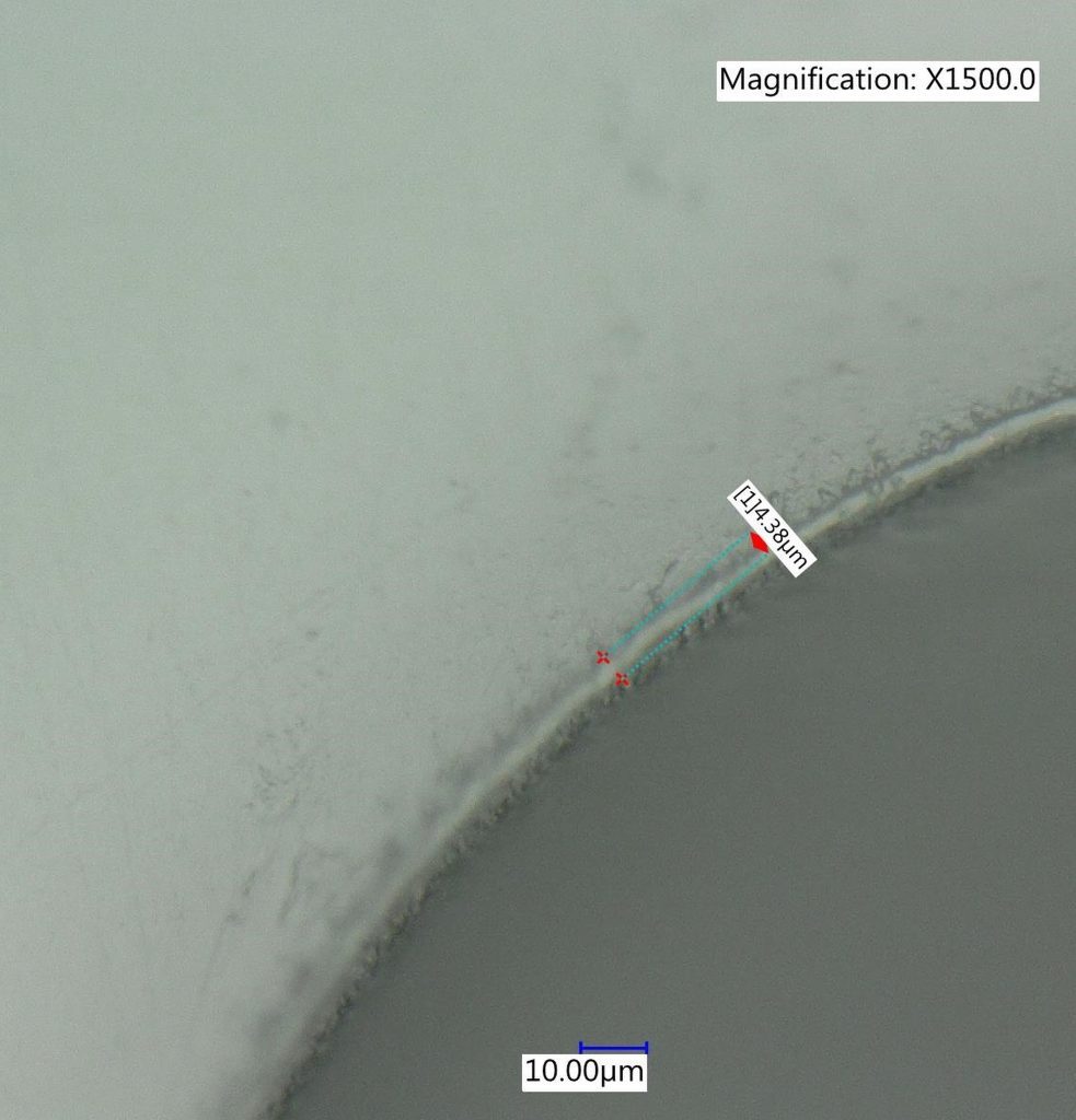
Ultrafast lasers create smooth marks which can survive many cleaning cycles. During ultrafast laser marking, the laser removes no material, and there is no microcracking or surface damage.
The ultrashort pulses produce nanostructures on the surface of the medical device. These structures trap light and provide a high-contrast matt black “printed” appearance. You can see the marking from every angle.
The markings are smooth to the touch and do not cause biological traps.
Download this application note as pdf.
Summary
The ultrashort pulses delivered by NKT Photonics’ ultrafast laser range are well suited to marking in the medical industry and fulfilling the requirements for UDI-compliant marking.
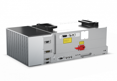
The ORIGAMI XP is the first all-in-one, single-box, microjoule femtosecond laser on the market. The laser head, controller, and air-cooling system are all integrated into one small and robust package, with a footprint so small it even fits into a hand-luggage!